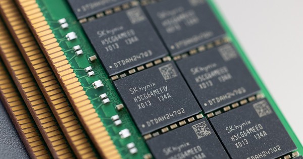
SK Hynix: The Chosen Stock by Nvidia and a $10 Billion Investment
The world of advanced chip packaging is experiencing significant growth, with increasing demand for high-bandwidth memory (HBM) in the development of artificial intelligence (AI). SK Hynix, a leading player in the industry, recognizes the importance of meeting this growing demand and has invested over $1 billion in expanding and improving its chip production process at its headquarters in Icheon, South Korea.
Led by Lee Kang-Wook, a former engineer at Samsung Electronics, SK Hynix aims to innovate and solidify its position in the market. HBM, known as the most sought-after AI memory, plays a crucial role in improving energy efficiency and performance. SK Hynix has expertise in advanced semiconductor interconnect technology, making it the prime choice for Nvidia.
Nvidia’s decision to select SK Hynix as their HBM supplier has significantly boosted the Korean company’s value to 119 trillion won. This increase of nearly 120% in stock price since the beginning of 2023 has placed SK Hynix ahead of its competitors, including Samsung and Micron Technology.
At 55 years old, Lee is a pioneer in the field of third-generation packaging technology, known as HBM2E. His innovative approach caught Nvidia’s attention in late 2019. Lee’s passion lies in the process of stacking chips to achieve higher performance. His expertise in 3D integration technology, acquired during his Ph.D. at Tohoku University in Japan, led to the development of HBM, which has become the foundation of SK Hynix’s success.
SK Hynix’s major investments are focused on advancing MR-MUF and TSV technologies. In contrast, Samsung, preoccupied with succession issues, struggles to keep up. Last year, Nvidia agreed to use Samsung’s HBM chip. On February 26, Samsung announced the development of HBM3E, the fifth-generation technology, featuring 12 layers of DRAM chips and the industry’s largest capacity of 36GB.
Lee is optimistic about SK Hynix’s prospects amidst fierce competition and considers the current investment as a foundation to meet future HBM requirements. Notably, industry reports reveal SK Hynix and other leading Korean tech companies are planning to invest $471 billion to establish the world’s largest chip production center.
The Korean government has detailed plans for this venture, including funding for 13 chip factories and three new research facilities. The supercluster will stretch from Pyeongtaek to Yongin, with a monthly wafer capacity of 7.7 million, starting in 2030.
The competition for semiconductor supremacy is intensifying globally. Neighboring regions such as Japan and Taiwan are actively investing in memory chips. South Korea’s ambitious plan aims to encompass material suppliers and small-scale chip designers, ultimately increasing self-sufficiency in the semiconductor supply chain from 30% to 50% by 2030.
Pangyo, a hub for leading tech companies, will produce high-performance AI chips, while Suwon will serve as a complex semiconductor testing center. Pyeongtaek will focus on researching and developing new semiconductors at the Advanced Institute of Science and Technology.
President Yoon Suk Yeol emphasizes that domestic nuclear power plants will provide stable electricity for the new chip production cluster, attracting foreign investment opportunities.
SK Hynix’s commitment to expanding and enhancing domestic technology capabilities positions it as a key player in the global semiconductor industry. With a strong focus on innovation and investment, SK Hynix strives to meet the growing demands of the market and maintain its competitive edge.
This article was originally published on Business Today.

